- 您现在的位置:买卖IC网 > Sheet目录511 > SI5853CDC-T1-E3 (Vishay Siliconix)MOSFET P-CH 20V 4A 1206-8
�� �
�
�Si5853CDC�
�Vishay� Siliconix�
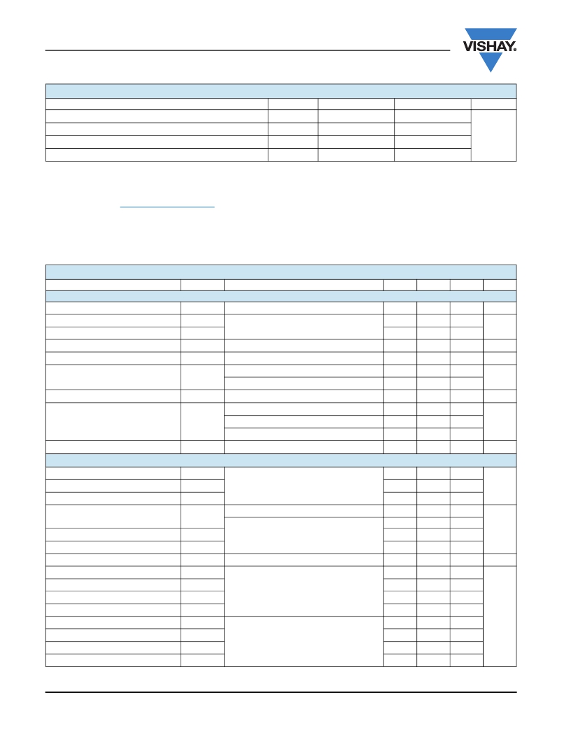
�THERMAL� RESISTANCE� RATINGS�
�Parameter�
�Symbol�
�Typical�
�Maximum�
�Unit�
�Maximum� Junction-to-Ambient�
�(MOSFET)� b,� c,� f�
�R� thJA�
�70�
�85�
�Maximum� Junction-to-Foot� (Drain)� (MOSFET)�
�Maximum� Junction-to-Ambient� (Schottky)� b,� c,� g�
�Maximum� Junction-to-Foot� (Drain)� (Schottky)�
�R� thJF�
�R� thJA�
�R� thJF�
�33�
�85�
�40�
�40�
�105�
�50�
�°C/W�
�Notes:�
�a.� Package� limited.�
�b.� Surface� mounted� on� FR4� board.�
�c.� t� ≤� 5� s.�
�d.� See� Solder� Profile� (� www.vishay.com/doc?73257� ).� The� ChipFET� is� a� leadless� package.� The� end� of� the� lead� terminal� is� exposed� copper� (not�
�plated)� as� a� result� of� the� singulation� process� in� manufacturing.� A� solder� fillet� at� the� exposed� copper� tip� cannot� be� guaranteed� and� is� not�
�required� to� ensure� adequate� bottom� side� solder� interconnection.�
�e.� Rework� conditions:� manual� soldering� with� a� soldering� iron� is� not� recommended� for� leadless� components.�
�f.� Maximum� under� steady� state� conditions� for� MOSFETs� is� 120� °C/W.�
�g.� Maximum� under� steady� state� conditions� for� Schottky� is� 125� °C/W.�
�SPECIFICATIONS� T� J� =� 25� °C,� unless� otherwise� noted�
�Parameter�
�Symbol�
�Test� Conditions�
�Min.�
�Typ.�
�Max.�
�Unit�
�Static�
�Drain-Source� Breakdown� Voltage�
�V� DS� Temperature� Coefficient�
�V� GS(th)� Temperature� Coefficient�
�V� DS�
�Δ� V� DS/TJ�
�Δ� V� GS(th)/TJ�
�V� GS� =� 0� V,� I� D� =� -� 250� μA�
�I� D� =� -� 250� μA�
�-� 20�
�-� 20�
�2.1�
�V�
�mV/°C�
�Gate-Source� Threshold� Voltage�
�V� GS(th)�
�V� DS� =� V� GS� ,� I� D� =� -� 250� μA�
�-� 0.45�
�-1�
�V�
�Gate-Body� Leakage�
�Zero� Gate� Voltage� Drain� Current�
�On-State� Drain� Current� a�
�I� GSS�
�I� DSS�
�I� D(on)�
�V� DS� =� 0� V,� V� GS� =� ±� 8� V�
�V� DS� =� -� 20� V,� V� GS� =� 0� V�
�V� DS� =� -� 20� V,� V� GS� =� 0� V,� T� J� =� 85� °C�
�V� DS� ≤� -� 5� V,� V� GS� =� -� 4.5� V�
�V� GS� =� -� 4.5� V,� I� D� =� -� 2.5� A�
�-� 10�
�0.086�
�±� 100�
�-1�
�-� 10�
�0.104�
�nA�
�μA�
�A�
�Drain-Source� On-State� Resistance� a�
�R� DS(on)�
�V� GS� =� -� 2.5� V,� I� D� =� -� 2.1� A�
�0.120�
�0.144�
�Ω�
�V� GS� =� -� 1.8� V,� I� D� =� -� 0.5� A�
�0.170�
�0.205�
�Forward� Transconductance� a�
�g� fs�
�V� DS� =� -� 10� V,� I� D� =� -� 2.5� A�
�6�
�S�
�Dynamic� b�
�Input� Capacitance�
�C� iss�
�350�
�Output� Capacitance�
�Reverse� Transfer� Capacitance�
�C� oss�
�C� rss�
�V� DS� =� -� 10� V,� V� GS� =� 0� V,� f� =� 1� MHz�
�65�
�45�
�pF�
�Total� Gate� Charge�
�Gate-Source� Charge�
�Q� g�
�Q� gs�
�V� DS� =� -� 10� V,� V� GS� =� -� 8� V,� I� D� =� -� 2.9� A�
�V� DS� =� -� 10� V,� V� GS� =� -� 4.5� V,� I� D� =� -� 2.9� A�
�7.2�
�4.2�
�0.7�
�11�
�6.5�
�nC�
�Gate-Drain� Charge�
�Q� gd�
�1�
�Gate� Resistance�
�Turn-On� Delay� Time�
�Rise� Time�
�Turn-Off� Delay� Time�
�R� g�
�t� d(on)�
�t� r�
�t� d(off)�
�f� =� 1� MHz�
�V� DD� =� -� 10� V,� R� L� =� 4.4� Ω�
�I� D� ?� -� 2.3� A,� V� GEN� =� -� 4.5� V,� R� g� =� 1� Ω�
�6.2�
�15�
�42�
�20�
�25�
�65�
�30�
�Ω�
�Fall� Time�
�Turn-On� Delay� Time�
�t� f�
�t� d(on)�
�10�
�5�
�15�
�10�
�ns�
�Rise� Time�
�Turn-Off� Delay� Time�
�Fall� Time�
�t� r�
�t� d(off)�
�t� f�
�V� DD� =� -� 10� V,� R� L� =� 4.4� Ω�
�I� D� ?� -� 2.3� A,� V� GEN� =� -� 8� V,� R� g� =� 1� Ω�
�15�
�20�
�10�
�25�
�30�
�15�
�www.vishay.com�
�2�
�Document� Number:� 69774�
�S10-0547-Rev.� B,� 08-Mar-10�
�发布紧急采购,3分钟左右您将得到回复。
相关PDF资料
SI5853DDC-T1-E3
MOSFET P-CH D-S 20V 1206-8
SI5855CDC-T1-E3
MOSFET P-CH/SCHOTTKY 20V 1206-8
SI5857DU-T1-GE3
MOSFET P-CH D-S 20V PPAK CHIPFET
SI5858DU-T1-GE3
MOSFET N-CH 20V 6A PPAK CHIPFET
SI5903DC-T1-GE3
MOSFET DUAL P-CH 20V 2.1A 1206-8
SI5905BDC-T1-GE3
MOSFET DUAL P-CH D-S 8V 1206-8
SI5915BDC-T1-GE3
MOSFET P-CH 8V CHIPFET 1206-8
SI5915DC-T1-GE3
MOSFET 2P-CH 8V 3.4A 1206-8
相关代理商/技术参数
SI5853DC
制造商:VISHAY 制造商全称:Vishay Siliconix 功能描述:P-Channel 1.8-V (G-S) MOSFET With Schottky Diode
SI5853DC-T1
功能描述:MOSFET 20V 3.6A 2.1W RoHS:否 制造商:STMicroelectronics 晶体管极性:N-Channel 汲极/源极击穿电压:650 V 闸/源击穿电压:25 V 漏极连续电流:130 A 电阻汲极/源极 RDS(导通):0.014 Ohms 配置:Single 最大工作温度: 安装风格:Through Hole 封装 / 箱体:Max247 封装:Tube
SI5853DC-T1-E3
功能描述:MOSFET 20V 3.6A 2.1W RoHS:否 制造商:STMicroelectronics 晶体管极性:N-Channel 汲极/源极击穿电压:650 V 闸/源击穿电压:25 V 漏极连续电流:130 A 电阻汲极/源极 RDS(导通):0.014 Ohms 配置:Single 最大工作温度: 安装风格:Through Hole 封装 / 箱体:Max247 封装:Tube
SI5853DDC
制造商:VISHAY 制造商全称:Vishay Siliconix 功能描述:P-Channel 20-V (D-S) MOSFET with Schottky Diode
SI5853DDC-T1-E3
功能描述:MOSFET 20V 4.0A 3.1W 105mohm @ 4.5V RoHS:否 制造商:STMicroelectronics 晶体管极性:N-Channel 汲极/源极击穿电压:650 V 闸/源击穿电压:25 V 漏极连续电流:130 A 电阻汲极/源极 RDS(导通):0.014 Ohms 配置:Single 最大工作温度: 安装风格:Through Hole 封装 / 箱体:Max247 封装:Tube
SI5855CDC
制造商:VISHAY 制造商全称:Vishay Siliconix 功能描述:P-Channel 20-V (D-S) MOSFET With Schottky Diode
Si5855CDC-T1-E3
功能描述:MOSFET 20V 3.7A 2.8W 144mohm @ 4.5V RoHS:否 制造商:STMicroelectronics 晶体管极性:N-Channel 汲极/源极击穿电压:650 V 闸/源击穿电压:25 V 漏极连续电流:130 A 电阻汲极/源极 RDS(导通):0.014 Ohms 配置:Single 最大工作温度: 安装风格:Through Hole 封装 / 箱体:Max247 封装:Tube
SI5855CDC-T1-GE3
制造商:Vishay Semiconductors 功能描述: